

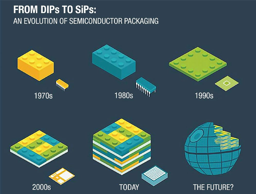
Packaging technology for semiconductor devices is complex and varied. Hermetically sealed ceramic packages with wire bonded die are still commonly used in high reliability space missions. However, this style of packaging has long ago disappeared from commercial applications. Driven by lower cost, lighter weight, reduced power, and the need to pack more devices into ever smaller forms like cellular phones, many semiconductor packaging technologies are now considered assemblies or systems of chips.
Dual in-line packages (DIPs) gave way to flip chip devices of the 1990s. High-density substrates, redistribution layers through silicon vertical interconnect accesses (vias), and different types and sizes of bumps now define the modern System in Package (SiP) landscape.
Assurance processes to characterize this modern generation of packaging technologies has shifted substantially from the end user to the vendor. End users still rely on historical component stress-based test approaches like temperature cycling, long-term high temperature life test, and humidity + bias testing to benchmark reliability. While providing an overall benchmark, such tests cannot guarantee coverage for all combinations of material and electrical interactions.
Modern SiP devices consist of multiple different size die with thousands of microbumps, various via technologies, and dozens of different dielectric layers. Known good die processes, built-in self-tests, and multiple wafer probing insertions require physics of failure-based design rules and formal tool suites. The goal is to adequately characterize the long-term performance and expected degradation of these state-of-the-art packages. These capabilities are an integral part of the design and manufacturing process and therefore reside with the vendors. Strategic partnerships with vendors are required to both obtain access to their capabilities as well as protect and manage the proprietary nature of this information.
The benefits of modern packaging technologies are profound for the space industry as 10 to 100 times reductions in size, weight, and power are now possible with 10,000 times improvements in processing capabilities. Effective assurance will require a new level of collaboration and intellectual property management to be successful.
This story appears in the September 2019 issue of Getting It Right, Collaborating for Mission Success.