

Failure analysis (FA) is the process of collecting and analyzing data to determine the mechanism and root cause of a part failure. The FA result may be sufficient to understand the root cause or it can be one of many data points that a multidisciplinary investigation team needs to systematically ferret out the anomaly.
The last 10 years have brought significant challenges to FA as technological complexity rapidly increased.
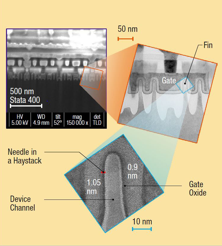
Modern fin field-effect transistor microcircuits can have over 10 billion transistors, up to 17 layers of interconnect, and wiring across a die footprint reaching 800mm2 (1.24in2). This results in hundreds of billions of potential fault locations where the defect may only be a few nanometers in size. Even a seasoned FA expert armed with standard sample preparation, optical imaging, static fault isolation, microprobing, scanning electron, and focused ion beam microscopy tools is challenged without adopting new techniques and tools.
To successfully deploy these modern technology products, the design must include “Design for Testability” diagnostics for failure location, i.e., a “map” to a group of components (netlists) or to a specific transistor: the street address of the defect. Automated test equipment dynamically communicates with fault isolation systems to bound the anomaly location into a reasonable search area for physical deconstruction.
The physical deconstruction process leverages computer-aided design to overlay the failing netlists and narrow down the failure location. In addition to a scanning electron microscopy inspection at each layer, conductive atomic force microscopy and electrical nanoprobing are conducted to further physically isolate the defect. After isolation is adequately completed, a focused ion beam system is used to create a ~20nm-thick transmission electron microscopy sample containing the defect to analyze.
Custom microcircuit design on advanced modern semiconductor technologies requires enabling FA capabilities in the circuit design phase. Modern FA techniques may require custom fixturing, which can take up to six months’ lead time to design and build. Early interaction between designers, foundries, and FA teams is critical to ensure the right capabilities are accessible.
The writing and publication of the paper underpinning this article was supported by the Jet Propulsion Laboratory (JPL), California Institute of Technology (Caltech), under a contract with NASA. Any reference herein to any specific commercial product, process, or service by trade name, trademark, manufacturer, or otherwise does not constitute or imply its endorsement by the United States government or JPL/Caltech.
This story appears in the September 2019 issue of Getting It Right, Collaborating for Mission Success.